


In 2012, Kodak officially filed a bankruptcy protection application to the Manhattan Court of the United States, which got lots of attention and discussions at home and abroad. It was unexpected that Kodak, founded in 1880, as the leader of global image product industry, would collapse in just a few years. Since then, the film camera and film produced by Kodak has gradually become history for a generation of people.
")
The fall of Kodak indicates an update to the entire image product market. The 21st century has witnessed the astonishing development of digital imaging technology and its quick replacement of film imaging technology to be the well-deserved king of the image market. It is the rise of image sensing technology that helps promote the industrial transformation.
The origin of image sensing
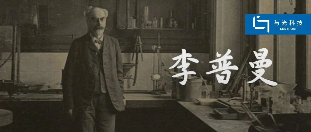
Image sensing technology is closely connected with the discovery of photoelectric effect. In December 1886, Heinrich Rudolf Hertz, a German physicist, by accident, found in an experiment that when ultraviolet rays were irradiated onto the metal surface, the metal would emit electric particle current. This strange phenomenon is later known as photoelectric effect. In March 1905, Albert Einstein, a Jewish physicist, explained photoelectric effect and listed the photoelectric effect equation in a creative way by combining the theory of relativity with light quantum theory. He was awarded the Nobel Prize for Physics for the creative explanation.
")
Figure 2. Heinrich Rudolf Hertz and photovoltaic effect principle
")
The birth of image sensor
With continuous research supported by Russia and American scientists, Radio Corporation of America (RCA) invented the world's first Photo Multiplier Tube (PMT) in 1936, which marks the formal advent of image sensor. PMT can convert extremely weak optical signals to electrical signal output and amazingly multiply the electronic ability. So far it has played an important role in space research, medicine, biology, astronomy, chemistry.
")
CCD goes to the market
It is the invention of Charge Coupled Device (CCD) that brings image sensors into public's vision. In 1969, Bell Labs in the United States was working hard on video phone and semiconductor bubble memory technology. Willard Boyle and George Smith, Scientists at Bell Labs, creatively made a device that could transfer charges along the surface of a piece of semiconductor by combining the two technologies, which is called Charge 'Bubble' Devices (CBD). In the follow-up experiments, they found that the photoelectric effect can generate charges on the surface of such components to form digital images, so they came up with the idea of using inductive coupling devices to capture images; after countless experiments, in 1971, they finally captured the image by adopting a simple linear device. The CCD was born.
")
In 1973, Fairchild Corporation of the United States produced the first commercial CCD image sensor, which marked CCD formally went from the laboratory to the market and entered a practical stage; in 1975, Kodak Corporation made the world’s first digital camera with 201100 CCD produced by Fairchild Corporation, launching the digital era of imaging products. Unfortunately, Kodak did not value the development and market expansion of digital camera. It still focused on the market development of film camera, and ultimately lost the vast market of imaging products.
")
Figure 6. The first commercial CCD(Fairchild, USA)
")
At the end of the 20th century, with the rapid development of the integrated circuit, CCD has been rapidly improved in terms of performance. In 1978, Sony produced a CCD with 120,000 pixels, and in 1980 released the world’s first commercial mass-produced 120,000-pixel CCD color camera (XC-1); with success in XC-1, in 1981, Sony released a color CCD camera with 279,000 pixels (Mavica Camera). The mature miniaturization design and high image quality of Mavica Camera stress the huge potential of CCD in the field of photography. Then companies like Pentacon (Germany), Panasonic (Japan), Fujifilm, Minolta, all invested in the development of CCD camera, and successively launched their own CCD cameras. This also accelerated the advancement of CCD technology. In 1986, CCD exceeded 1 million pixels, reaching 1.4 million; in 1991, CCD, with 4 million pixels, began to achieve mass production.
")
With the improvement of CCD imaging quality and the production technology, the market share of digital camera increased sharply. In 1996, the global output of digital camera was about 1 million units. In 2000, it reached 10 million units, which surged 10 times in just 5 years. The prospects of digital camera are extremely broad.
Entering the 21st century, CCD gained a lot of glory in the first few years. Thanks to the improvement of CCD performance and the decline in price, affordable and high-performance digital camera truly became popular. Digital cameras like Minolta DIMAGE7, Sony F707, Canon G2, Casio QV4000 stood out together and occupied a huge market. Behind the prosperity of the CCD imaging market, CMOS (Complementary Metal Oxide Semiconductor) image sensors were quietly rising.
The rise of CMOS
CMOS is an abbreviation for complementary metal oxide semiconductor, and its production technology is the same as that of integrated circuits such as computer chips and storage devices. The rise of CMOS benefits from the rapid development of the integrated circuit industry. In 1963, C.T.Sah and Frank Wanlass of Fairchild Semiconductor Corporation submitted a paper on CMOS technics, and proposed CMOS technology for the first time in the semiconductor industry. In 1968, Albert Medwin research team from Radio Corporation of America developed the world's first CMOS integrated circuit. In the 1970s, the continuous development of advanced lithography technology greatly improved the CMOS technology, and the CMOS size entered the sub-micron stage. In the 1990s, technics like Shallow Trench Isolation (STI) and Salicide began were applied to CMOS. The CMOS technology was continuously updated and the feature size continued to shrink.
")
Since the birth of CMOS, its feature size has been developing as predicted by "Moore's Law" proposed by Gordon Moore, one of the founders of Intel. Moore's Law refers to Gordon Moore's perception that the number of transistors on a microchip doubles every 18 -24 months and the performance will double accordingly, though the cost of computers is halved. In 1999, the feature size of CMOS was 180nm, and in 2009 it reached 32nm. In ten years, a CMOS chip of the same size has been integrated nearly 32 times.
")
CMOS Image Sensor (CIS) is an image sensor made with CMOS technology. Entering the 21st century, due to the rapid development of CMOS technology, the performance of CIS has gradually reached and surpassed CCD, becoming the mainstream of the image sensor consumer market. In 2000, Canon launched the first digital SLR camera D30 with CIS chip, making it possible for CIS to replace CCD; in 2002, Canon launched the first full-frame digital SLR camera 1Ds with CIS, which enjoys 1140 Megapixels. It has a favorable price advantage compared with similar products, so it became popular quickly and achieved market success. In 2007, the CIS-based SiimpelAF camera model was successfully developed, and marked a major breakthrough in camera miniaturization. Digital camera entered the chip era. Statistics from Frost&Sullivan shows that, in 2012, the global image sensor market reached 9.96 billion U.S. dollars, of which CIS accounted for 55.4% and CCD accounted for 44.6%. In 2019, the global image sensor market grew to 19.87 billion U.S. dollars, of which CIS accounted for 83.2%. Its market scale far exceeded CCD.
")
Figure 11. Canon D30 (the left one) and Canon 1Ds (the right one)
")
Figure 12. Siimpel AF camera model
")
CIS becomes mainstream
Why can CIS quickly replace CCD in just a few years and become No. 1 in the field of image sensors?
The first is about the cost. The circuits and components in CCD are integrated on semiconductor single crystal materials that are complicated in the production. Only a few manufacturers in the world such as Dalsa, Sony, and Panasonic can produce CCD wafers, and the cost is relatively high; however, CIS is integrated on metal oxide semiconductor materials, and its manufacturing process is the same as that of semiconductor integrated circuits like computer chips and storage devices. The technic is simple and the cost is low. Therefore, for the same performance, the cost of CIS is much lower than that of CCD.
The second is about integration. CCD can only output analog electrical signals. It is necessary to add subsequent address decoders, analog converters, image signal processors, and to provide three sets of power synchronization clock with different voltages to control circuits, so the integration is extremely low; while CIS adopts an integrated circuit craft that can integrate all modules on a chip, the integration level is very high. Besides, compared with CCD, CIS has a higher readout rate and lower power consumption, it is more suitable for portable devices such as mobile phones and digital cameras.
Due to the low cost, small size, high speed and low power consumption, CIS has become the mainstream of the image sensor market and is widely used in camera, mobile phone, aerospace, military, security monitoring, vehicle camera, endoscopic camera. According to "A Report on 2020-2024 CIS Image Sensor Industry Market In-depth Research and Investment Prospect Analysis ", from 2013 to 2019, the global CIS has a compound annual growth rate of 15.2% in shipment and of 13.1% in sales, showing a trend of rapid growth; in 2019, global CIS reached 6.09 billion units in shipment and reached 15.47 billion U.S. dollars in sales. It is estimated that by 2024, global CIS will reach more than 10 billion in shipment and more than 23 billion U.S. dollars in sales.
")
With the advancement of photolithography technology and production technics, CIS pixel size is further reduced, and it is also combined with other advanced technologies such as chip stacking. In 2012, Sony introduced a two-layer stacked image sensor; in 2018, Samsung and Sony developed a three-layer stacked image sensor. Chip stacking that can layer the sensing function and processing function of CIS reduce the chip size, provide large-scale parallel signal transmission, and realize high-speed reading and writing of all pixel data of the image sensor. These features meet the needs of autonomous driving, medical imaging and high-end photography. The application of CIS in these emerging fields has promoted the original innovation of CIS technology and offered continuous impetus for the development of vision technology.