


Recently, Seetrum has completed its hundred-million-yuan Series A and Series A+ financing rounds. The investment consortium is led by Sunny Optical Technology, with continued participation from existing investors Xinyi Capital, Guanxin Investment, Zhongqiao Venture Capital, and Jingguang Co-Innovation Fund. Proceeds from this financing will be allocated to mass production and technological upgrades of computational spectral chips to consolidate the core business of consumer electronics imaging. More importantly, the funds will fuel the R&D of physical AI vision chips, building hardware perception gateways for spatial intelligence and world models. Rooted in computational optics and micro-nano optics technologies, the company will gradually establish an optical chip platform for next-generation intelligent terminals, paving a full technical pathway from spectral sensing to multi-dimensional physical vision.
Physical AI Vision Chips: Opening the Gateway to the Physical World for AI
Four Waves of AI Evolution
The evolution of AI can be viewed as a gradual progression of machine capabilities to integrate with and interact with the physical world:
Perception AI: The earliest phase centered on environmental information interpretation, including image recognition and speech comprehension.
Generative AI: A transformative leap where AI generates text, images, and synthetic audio.
Agentic AI: The current advanced stage, where AI acts as intelligent assistants embedded in workflows, capable of end-to-end tasks spanning comprehension, coding, and execution. As Jensen Huang noted in his recent GTC keynote: “Agents go to work — AI can reason, plan, generate code, call tools, and deliver tangible outputs.”
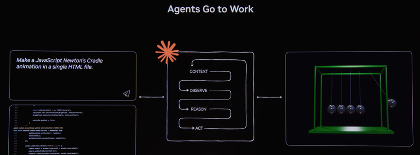
Source: NVIDIA
Physical AI: The upcoming frontier where AI breaks free from digital screens to interact with the tangible physical world. This paradigm demands an ability to interpret 3D space, perceive dynamic environments in real time, assess physical changes accurately, engage in physical interaction, and drive tangible hardware actions, marking the dawn of the Physical AI era.
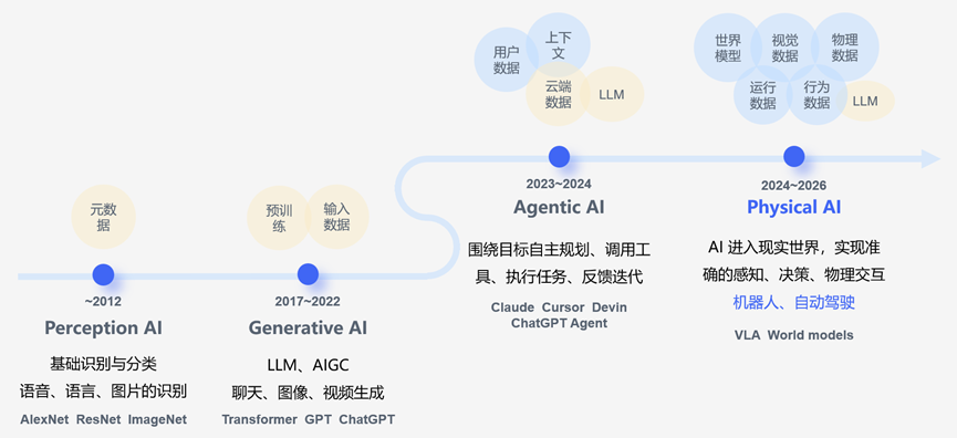
Four Waves of AI
Source: Compiled by Seetrum
Defining Physical AI
Prior generations of AI largely operated within purely digital domains. Physical AI, by contrast, solves real-world problems and delivers stable performance via physical hardware carriers. It refers to an integrated AI system combining sensor clusters, intelligent agents, hardware carriers, and environmental perception, capable of forming a closed loop of perception, cognition, decision-making, and execution — closely aligned with embodied intelligence. Beyond a digital "brain", Physical AI systems possess a physical "body" to interact with real environments.
The operating workflow of Physical AI begins with raw physical world sensing. Sensor clusters extract environmental feature data, AI models conduct predictive reasoning and decision-making, and execution hardware acts back upon the physical world, forming a complete closed loop of perception, decision, and action.
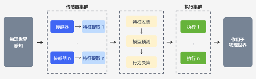
Workflow of Physical AI
Source: Physical artificial intelligence (PAI): the next-generation artificial intelligence, Compiled by Seetrum
From a global industrial perspective, major tech giants are heavily investing in Physical AI, confirming it as an irreversible high-growth track:
-- Meta filed patents for AR/VR eye-tracking solutions leveraging polarization devices, delivering high-precision, low-power 3D ocular sensing via liquid crystal polarization holography.
-- Google DeepMind launched Gemini Robotics (VLA) and Gemini Robotics-ER (VLM), boosting robots’ spatial and visual reasoning capabilities to complete complex physical manipulation tasks.
-- NVIDIA released the Cosmos model, integrated with the Omniverse platform to build a full-stack Physical AI infrastructure covering model training, validation, and deployment.
-- NVIDIA partnered with Unitree Robotics to launch the H2 Plus humanoid robot reference design embedded with proprietary models and computing platforms, deepening ecosystem deployment across Physical AI and humanoid robotics.
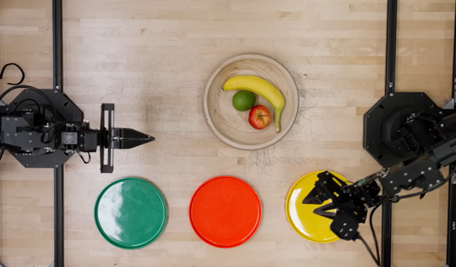
Training Gemini Robotics to Sort Fruits into Color-Coded Trays
Source: Google DeepMind
When AI must observe, interact with, and alter the physical world, demand for richer, more complex real-world data surges. Real-time, high-fidelity physical data becomes the foundation of system performance. Competition in AI is no longer limited to model architecture and computing scale — it hinges equally on perception performance. For real-world robotic and industrial tasks, low-power, high-frame-rate, robust sensing that delivers actionable data for spatial reasoning and decision-making emerges as a core competitive advantage.
Why Start with Vision Sensing
Unlike traditional AI paradigms that rely on massive datasets and backend deep learning computation, Physical AI is defined by deep integration between intelligence and the tangible world. It depends on native raw physical data and physical hardware carriers, using multi-modal sensing (vision, tactile, etc.) to interpret real environments.
Vision stands out as the most critical information input channel: humans acquire over 80% of external sensory data through sight. For machines, vision forms the foundational capability for environmental recognition, target detection, spatial relationship judgment, and motion decision-making — indispensable for autonomous vehicles, industrial robots, and automated control systems. This is why Seetrum chose Physical AI vision chips as its core entry point.
This direction aligns perfectly with the core breakthroughs of World Models and Spatial Intelligence. As AI migrates from virtual simulations to real-world tasks, World Models require high-quality, continuous environmental sensing data to model temporal-spatial relationships and physical causality. This addresses critical pain points plaguing real-world AI: low sample efficiency, limited planning capacity, and prohibitive trial-and-error costs. Machines must not only identify objects but also gauge their position, distance, motion, surface material, and predict subsequent physical changes. In this context, vision chips are redefining their value proposition: they deliver low-redundancy, high-efficiency front-end data streams that serve as foundational hardware support for spatial intelligence and World Models.
Entering World Models via Vision
Source: AI-Generated
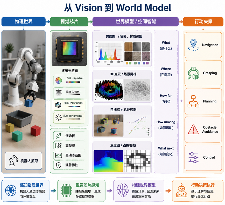
Physical AI Vision Chips
Drawing inspiration from biological vision, a research team led by Professor Huang Yidong (Seetrum founder, Tsinghua University) and Associate Professor Cui Kaiyu proposed the Spectral Convolutional Neural Network (SCNN) architecture. The design integrates massive micro-nano modulation structures directly atop CMOS image sensors, enabling the sensor to function simultaneously as the input layer and the first convolutional layer. It performs large-scale parallel vector inner product calculations across the spectral dimension, paired with lightweight subsequent electrical convolutional layers to form an efficient optoelectronic hybrid neural network.
Building on this architecture, the team developed spectral perception chips capable of processing raw natural imagery. These chips deliver massively parallel computation across millions to hundreds of millions of spatial pixels, while extracting material composition data via continuous spectral dimension analysis to dynamically identify object components and map physical features — enabling in-sensor edge computing. Relevant research findings were published in the top international journal Nature Communications.
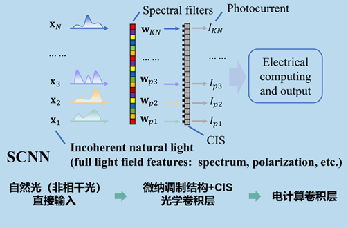
Spectral Convolutional Neural Network (SCNN) Architecture
Source: Cui, K. et al., Nature Communications 16, 81 (2025)
Leveraging this computational perception framework, Seetrum develops multi-scenario hardware sensors for material identification and multi-modal perception, paired with proprietary backend algorithm stacks to address diverse complex industrial requirements. The company is currently conducting joint pre-research with leading smartphone OEMs to commercialize these technologies.
In the next phase, Seetrum will target critical hardware gaps in Physical AI through R&D of multi-dimension integrated Physical AI vision chips. Positioned as the company’s new strategic pillar, these chips will expand commercial reach beyond consumer electronics into embodied intelligence and smart manufacturing.
Computational Spectroscopy: Structural Color Paves the Way for Next-Generation High-Performance Imaging
Commercialization of Mobile Imaging Products
Since its founding, Seetrum first achieved commercial traction for spectral chips in consumer electronics. Addressing demand for superior color reproduction in smartphone imaging, the company deeply integrates chip and algorithm capabilities to build differentiated strengths in color rendition, regional color temperature detection, and automatic white balance (AWB) optimization. This creates an end-to-end technical closed loop spanning chips, algorithms, and applications. Multiple product lines have been adopted by top smartphone manufacturers, reaching shipment volumes of 10 million units.
The mass-market deployment of computational spectral chips validates Seetrum’s ability to translate complex optical technologies into large-scale consumer products, while proving its robust engineering and mass production capabilities.
Three Generations of Spectral Chip Technology Evolution
The spectral chip industry has evolved from single-point sensing to multi-spectral imaging. Material color filters dominated traditional solutions but now face inherent performance and design bottlenecks. Meanwhile, structural color modulation technology has matured for mass production, offering superior spectral tuning, programmable flexibility, and deeper synergy with spectral algorithms — emerging as the optimal pathway for next-generation multi-spectral imaging.
Core Principles: Structural Color vs. Material Color
Structural Color: Relies on micro-nano optical structures (photonic crystals, metasurfaces, Fabry-Pérot resonators) to manipulate light via interference, diffraction, and scattering to generate color.
Material Color: Uses chemical pigments and dyes to selectively absorb and reflect light to produce color.
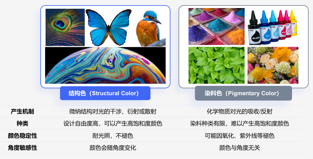
Comparison Between Structural Color and Material Color
Source: Seetrum
The evolution of spectral imaging technology for smartphones unfolds across three distinct stages:
-- Single-point color temperature sensors: Deploy discrete narrowband filters to detect color temperature, delivering improved spectral modulation and AWB accuracy compared to standard RGB CIS sensors. First featured on the iPhone X, these sensors are widely adopted in mid-to-high-end Android flagships. Core limitation: inability to capture full imaging data.
-- Material color multi-spectral imaging: Uses dye filter arrays paired with spectral reconstruction algorithms to capture snapshot multi-spectral data, bringing laboratory-grade multi-spectral imaging to consumer smartphones. However, dye-based material filters suffer from overlapping spectral channels and limited spectral modulation performance, yielding marginal improvements in AWB precision relative to RGB CIS sensors. The industry is actively exploring alternative technologies to meet stricter demands for spectral tuning, independent optical channels, and algorithm compatibility.
-- Structural color multi-spectral imaging: Integrates micro-nano structured filter arrays with spectral reconstruction algorithms. Subwavelength light field modulation enables precise spectral encoding of incoming light to capture high-fidelity snapshot multi-spectral data. Structural color technology delivers clear advantages in spectral selectivity, independent optical channels, and design flexibility, drastically boosting sensor spectral modulation performance and AWB accuracy.
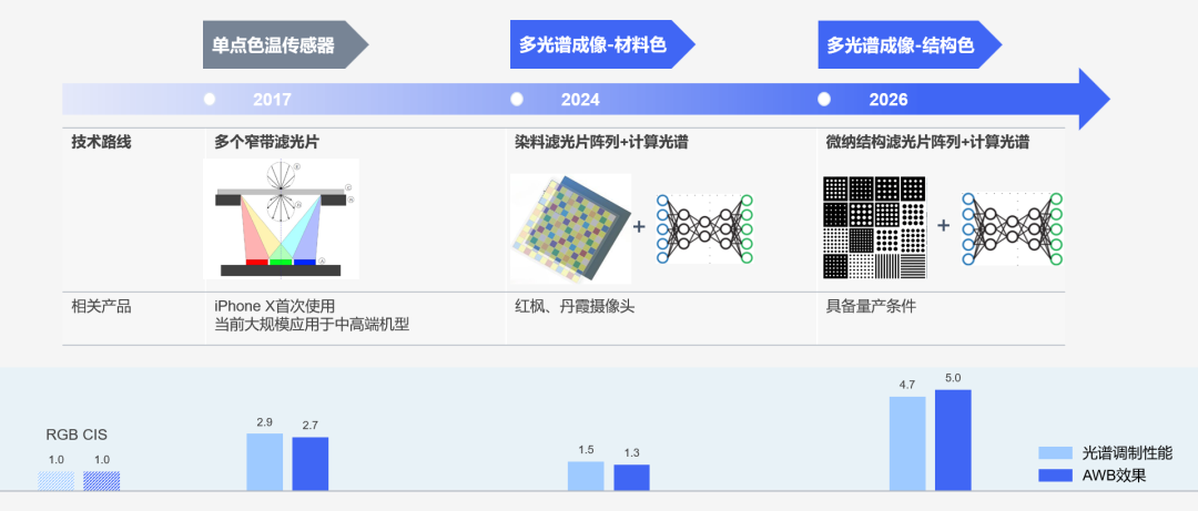
Development Path of Spectral Chips in Smartphone Imaging
Source: Seetrum
Seetrum has completed technical upgrades to its structural color spectral modulation solutions, with products ready for mass production. Hardware-software co-optimization has resolved the longstanding pain point of angular sensitivity in structural color sensors. Micro-nano structures enable ultra-fine spectral control with exceptional design freedom, unlocking substantial performance gains for end-user devices. High-performance spectral modulation via micro-nano structures represents an inevitable evolution trajectory for spectral chips and will remain Seetrum’s core competitive edge for sustained product leadership.
Strategic Vision: Embracing the Convergence of Photonics and AI
Seetrum’s founding team boasts over two decades of foundational expertise in computational and micro-nano optics. Building on breakthrough research in light field manipulation, micro-nano structure design, optical information acquisition, and computational imaging, the company has established systematic capabilities spanning chip design, component manufacturing, algorithm development, and end-user application — continuously translating cutting-edge optical chip research into commercialized products.
The company advances along a clear dual technical roadmap:
-- Iterate and upgrade computational spectral chips to build differentiated hardware and algorithm solutions;
-- Commercialize Physical AI vision chips to deliver foundational hardware for spatial intelligence and World Models.
Photonics is reshaping how machines capture and process information, while AI unlocks machines’ capacity to understand and interact with the physical world. Standing at the intersection of these two transformative technological waves, Seetrum will drive collaborative innovation across computational optics, micro-nano optics, and intelligent algorithms. The company aims to fully seize industrial opportunities arising from photonics-AI convergence, empowering industrial intelligent upgrading and countless yet-to-be-defined future technology scenarios.